| > Kik Group | College of Optics and Photonics | UCF |
|
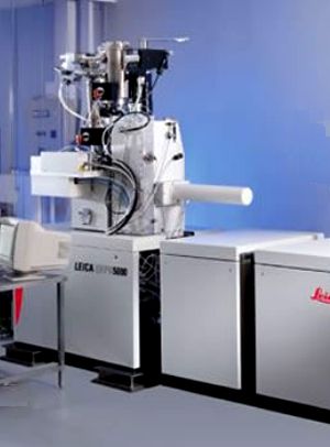
News DURIP Award for Mapping Spectroscopic Ellipsometer 2011 The NPNO group was awarded the ARO DURIP grant for a High-Speed Scanning Spectroscopic Ellipsometer for the Rapid Optical Mapping of Large-Area Plasmonic Nanocomposites. The system, manufactured by J.A. Woollam is a unique tool that allows for the rapid determination of the linear opical properties (refractive index, absorption coeffient, depolarization factors, anisotropy) in a wide wavelength range spanning the UV, VIS, and NIR ranges (210nm-1690nm). For more information on this instrument, please see the Laboratory page. 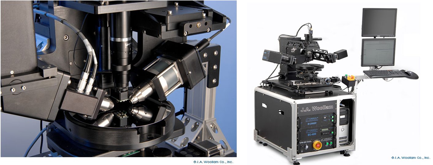 M2000 Spectroscopic Ellipsometer with focusing optics. Oleksandr Savchyn receives the CREOL Student of the Year Award. Thursday 4/2/2009 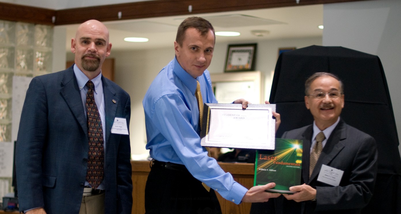 David Hagan, Oleksandr Savchyn, and Bahaa Saleh (Dean) during the award ceremony. On Thursday April 2 Oleksandr Savchyn received the 2008-2009 CREOL Student Of The Year Award for his research on silicon sensitization of of erbium in silicon-rich SiO2. The award was given for the high quality research as well as for his general dedication to science. As the winner of the award, Alex presented his research results in front of 150 visitors at the 2009 CREOL Affiliates Day. Alex' research topic focuses on the use of silicon nanocrystals as an optical sensitizer for erbium ions in silica. Erbium ions exhibit a well known optical transition at 1.5 um used for gain and lasing in the telecommunications industry. When Alex started his work it was commonly assumed that the effective optical absorption cross-section of erbium ions (Er3+) could be dramatically enhanced by co-doping Er doped SiO2 with silicon nanocrystals. A large collection of publications in top journals by many independent research groups appeared to support this view. While Alex' initial task was to optimize Er and Si doped SiO2 for gain applications, his consistently thorough data collection and analysis posed some difficult questions. The wealth of high-precision results on erbium and Si nanocrystal emission lifetimes, intensities, and absorption cross-sections that he collected pointed to a major problem with models proposed in the literature. Alex was able to take seemingly contradictory results and develop a new theory that attributes a large part of the Er sensitization to Si-related luminescence centers in the SiO2, not to Si nanocrystals as was previously thought. In a publication in Physical Review B, Alex and his collaborators at UCF demonstrated that this new model could account for many of the existing observations in the literature. His findings have recently been corroborated by an independent research group who used atom tomography to arrive at the same conclusion. Since his initial findings, Alex has published another extensive Physical Review B publication on the effect of hydrogen passivation on silicon-sensitized Er excitation in SiO2, as well as an Applied Physics Letters publication detailing the temporal dynamics of the Er excitation in this material. A fourth article is currently under review for publication in Applied Physics Letters, and additional studies on gain measurements on this material are ongoing. Importantly, his theory opens up new avenues for achieving optical gain in a silicon-based optical material, and will likely have a major impact on this research field. NSF CAREER Award for Nanophotonics and Near-field Optics group Thursday 2/1/2007 On February 1, 2007, the Nanophotonics and Near-field Optics group was awarded an NSF Career award for the program "CAREER: Silicon Compatible Hybrid Nanophotonic Systems". The NSF Faculty Early Career Development Program offers the National Science Foundation's most prestigious awards in support of junior faculty who exemplify the role of teacher-scholars through outstanding research, excellent education and the integration of education and research within the context of the mission of their organizations. The proposed work aims to advance the field of silicon photonics by taking advantage of the unique optical properties of nanostructured materials. Silicon photonics is a rapidly developing technology that will replace existing copper interconnects on computer chips with optical interconnects. This radical change in chip design promises to dramatically increase the performance of computers by increasing data transfer speeds and reducing the thermal load on electronic circuits. The success of silicon photonics relies on the integration of on-chip light sources and miniature optical waveguides. The main goals of this research program are the development of nanostructured semiconductor light sources and nanoscale metal waveguides for integration into the silicon photonics platform. The light source will consist of semiconductor elements and rare earth ions, embedded in silica based oxides. The electronic properties of the non-stoichiometric oxides enables efficient excitation of the rare earth ions, resulting in the emission of 1.53 um light that can be used to transport information. Additionally, nanoscale waveguides based on the use of charge waves or surface plasmons will be fabricated. The hybrid integration of these two nanophotonic optical elements could play a central role in silicon photonics. Nanoscale focusing with 'perfect lens' demonstrated. Wednesday 11/08/2006 In 2000 it was predicted by Professor Pendry at Imperial College (UK) that a thin metal film could act as a unique type of lens that could produce images with a resolution better than the diffraction limit. The prediction appeared to contradict generally accepted theories, and caused significant discussion in the scientific community. In a recent experimental study Grady Webb-Wood performed direct measurements of the focusing effect using a thin gold film as the metal lens. In these studies the tip of a near-field microscope is used as a nanoscale light source. We demonstrate optimum focusing at a frequency coinciding with the localized surface plasmon wavelength, as predicted by theory. For more information, have a look at the article publications section. UCF participating in three new MURI awards Thursday 03/02/2006 Reported by the Florida Research Consortium: Governor Jeb Bush congratulated Florida's university-based research community on their outstanding performance in the 2006 Department of Defense (DoD) Multidisciplinary University Research Initiative (MURI) grant program. The University of Central Florida (UCF) received three of 30 grants awarded to 20 universities. The MURI grants awarded total more than $150 million, with Florida's grant contracts expected to be valued at approximately $15 million. [..] Two of the University of Central Florida awards came out of the Florida Photonics Center of Excellence; the third is from UCF's Institute for Simulation and Training. [.. At CREOL, one award including] Dr. Van Stryland as Principal Investigator, with Dr. Pieter Kik as co-PI, will study "Ultrafast Switching for Optical Imaging." Other institutions participating with CREOL as the lead are Georgia Institute of Technology, Purdue University, and University of Arizona. Additionally, Dr. Stryland is also a participant on a MURI award to Kent State, led by Dr. Palffy-Muhoray, to study Negative Index Materials. Read the full text (PDF) Near-field enhanced plasmon coupler explained Tuesday 08/04/2005 In today's plasmonics session at the SPIE conference in San Diego, Amitabh Ghoshal presented his simulation results of a nanostructure designed to interface effectively between a laser beam and tightly confined surface plasmons propagating along a metal surface. He showed that by placing an array of silver nanoparticles near a silver-SiO2 interface, one can coherently excite surface plasmons. Additionally he demonstrated that the excitation efficiency can be optimized by shape-tuning the local plasmon resonance of the nanoparticles. This type of resonantly tuned plasmon coupler can play the role of a 'optical bond pad' that links fiber optics to future plasmon integrated optical circuits. The article can be found in the publications section, and the presentation can be viewed and downloaded from the Talks page. New article on Si optical nanocrystal memory published Tuesday 09/28/2004 Today the results of an experimental study on a propotype Si based optical memory were published on the AIP website. The device makes use of the fact that light emission from Si nanocrystals can be turned off by charging the nanocrystals (adding electrons or holes). This phenomenon allows us to read out the charge state of a nanocrystal using optical methods. The nanocrystals in this study are embedded in a specially designed transistor gate stack, allowing for simultaneous optical and electrical access to the nanocrystals. To download the article, visit the publications section. Group celebrates one-year anniversary Wednesday 09/01/2004 Today marks the beginning of the second year of nanophotonics research in our group. In the past year we have grown from one employee to six group members, including the two latest additions to our group: Alex Savchyn and Forrest Ruhge. The coming year promises to be an exciting period for the group, with results from Amitabh's, Grady's, and Karthik's, projects coming in, and new research on integrated optical microlasers starting, including two enthusiastic new researchers to make this program a success. Congratulations to Grady for passing the Qualifier Exam! Thursday 08/26/2004 Passing the qualifier exam at CREOL is one of the major hurdles on the way to obtaining the Optics PhD. The qualifier is a two-day exam inlcuding problem sets from many areas in optics, including optical materials properties, interference and diffraction, geometrical optics, guided wave optics and more. To get a flavor of what we put our students through at the School of Optics, have a look at the qualifier exam requirements. Congratulations to Nanophotonics and Near-field Optics student Grady Webb-Wood for passing this grueling exam! Interactive class website based on SharePoint Monday 07/05/2004 This coming Fall term, the class Fundamentals of Optical Science taught by Prof. Kik will make use of SharePoint technology. This document sharing platform developed by Microsoft allows for a quick and easy setup of an interactive website, including message boards, polls, and more. The new class site is accessible to anyone at sharepoint.optics.ucf.edu . Depending on the outcome of this experiment a similar format may be adopted for other core courses taught at the College of Optics and Photonics in the near future. Joint project for UCF, UF, and Ocean Optics Wednesday 04/14/2004 Today it was officially announced that a team of researchers from UCF (Kik group, Dogariu group), UF Gainesville (Nishida group) together with Ocean Optics was selected by the Florida Photonics Center of Excellence to work on a joint research project on Tunable Plasmon Optical nanosensors for Biochemical Detection. The project has a one year duration with a possible extension to two years. Nanolunch celebrates its six-month anniversary Tuesday 04/04/2004 NanoLunch was started at the end of November in 2003 as a way for faculty to stay in touch with colleagues that are active in nanoscience. The lunch occurs every two weeks at noon, and is attended by people from various departments, including the School of Optics, Physics, Chemistry, and Mechanical, Materials and Aerospace Engineering. Present today were Kurt Busch, Pieter Kik, Stephen Kuebler, Eloy Hernandez, and Andy Winningham. UCF faculty that would like to know more, please see the NanoLunch info page Amitabh Ghoshal becomes Kik group's first e-beam lithography specialist Friday 03/12/2004 On Friday Amitabh Ghoshal completed an intensive two-week training session on the brand new Leica 5000+ e-beam lithography system which was recently installed in CREOL's 5000 sq. ft. cleanroom as part of the FPCE. The system will allow us to produce nanostructured samples over 600um x 600um areas with a spatial resolution better than 10 nm. Due to the sensitive nature of the equipment only a limited number of operators will be allowed to use the system. As one of these lucky few Amitabh Ghoshal will be our group's supplier of nanostructures for many (but not too many) years to come! Pieter Kik appointed as affiliate Professor of Physics Friday 02/27/2004 In today's faculty meeting at the Physics department, Pieter Kik was accepted as Affiliate Professor in Physics. This status strengthens the ties with the Physics department, and allows physics students to obtain their PhD in the Kik group. To read more about research in the Physics department, visit the Physics Homepage. New article on near-field focusing appears online Monday 01/26/2004 Today a theoretical study of near-field focusing by Kik, Maier, and Atwater was published on the AIP website. The article studies the regeneration of optical near-fields using surface plasmons at a metal-dielectric interface. Such near-field focusing could have applications in data storage, lithography, and near-field optical microscopy. To download the article, visit the publications section. Ocean optics donates equipment to Kik group Tuesday 12/10/2003 Ocean optics recently became an Industrial Affiliate of the School of Optics. Associated with this new relationship were equipment donations to several faculty at CREOL. Our group requested the DH2000 fiber coupled light source. This piece of equipment allows us to perform absorption measurements on small sample areas in our Near-field Optical Microscope. Students complete training on the NSOM Tuesday 11/25/2003 This week Matthias Kress from Witec visited CREOL to finalize the installation of our near-field scanning optical microscope (see our lab) and to instruct the students on the use of the microscope. The timing could not have been better: Grady, Amitabh, and Karthik could all attend, and heard the ins and outs of the microscope during the two day training session. Several test scans were completed successfully, and the system is now in full working order. Item America to aid Kik group in outfitting lab Monday 11/24/2003 After today's visit to the School of Optics, Manager Todd Hoffman of Item America agreed to assist the Kik group in designing equipment racks for the nanophotonics characterization lab. The racks will be built using the extensive selection of construction elements available from Item. The joint project will enable the group to set up high-end equipment racks at a significantly reduced cost, while giving Item the opportunity to learn about the specific requirements in an optics research environment. Kik group quadruples in size Monday 11/17/2003 Three students joined the group this week. Grady Webb-wood and Amitabh Ghoshal are joining as Graduate students in the group, and Karthik Narayanan joins for a six-month Master's thesis project. All three will initially work on projects involving surface plasmons. For info about the students, see the people section. Spectra Physics 2060-RS Kr laser arrives Monday 11/10/2003 The recently ordered Spectra Physics 2060-RS laser has arrived. The small-frame laser can emit lines from 350-800nm, giving us a broad range of wavelengths for plasmon excitation at metal surfaces. Output power will be in the 50+ mW range for each individual line. Workshop on High-Resolution Optical Microscopy Friday 10/24/2003 This workshop was co-organized by Witec, vendor of scientific equipment, and the Kik group at the School of Optics. In three thirty-minute talks the over fifty attendees heard about the ins and outs of several state-of-the-art microscopy techniques.
Dr. Klaus Weishaupt, co-founder of Witec
opened the workshop with an extensive overview of the Witec AlphaSNOM system, that enables the user
to do (among other things) Near-field Scanning Optical Microscopy, Confocal Microscopy,
and Atomic Force Microscopy. The second presentation was given by
Pieter Kik, who talked about
the special features that make NSOM a powerful tool for studying surface plasmons. In
the final talk of the day,
Prof. Kevin Belfield
discussed the most important characteristics of multi-photon fluorescence microscopy.
|