| > Kik Group | College of Optics and Photonics | UCF |
|
Publications The following is an overview of recent publications, including the full text in PDF format where possible. Please note: These articles may be downloaded for personal use only. Any other use requires prior permission of the author and the publisher. NEW Elimination of reflection losses in gradient metasurface optical elements Mengdi Sun and Pieter G. Kik, Appl. Phys. Lett. 124, 31701 (2024) [pdf] [link] Optical metasurfaces can achieve arbitrary wavefront control using subwavelength nanostructures, enabling imaging, sensing, and display applications using ultrathin structures. Metasurface optical elements that rely on propagation phase achieve this control using varying fill fractions of high refractive index materials, resulting in surface regions with significantly different effective refractive index. The intrinsic need for index variation makes it a non-trivial task to eliminate reflection losses across a complete optical element. Here, we investigate the optical performance of high-index metasurfaces, modified to suppress surface reflections. We demonstrate that a drastic reduction of surface reflections across an entire gradient metasurface is possible through the application of a single optimized anti-reflective layer with a thickness and refractive index that are substantially different from the traditionally expected values. NEW Diffractive light-trapping transparent electrodes using zero-order suppression Mengdi Sun, Di Huang, Pooria Golvari, Stephen M. Kuebler, Peter J. Delfyett, and Pieter G. Kik, Nanophotonics 12, 3545 (2023) [pdf] [link] A light-trapping transparent electrode design based on sub-surface binary dielectric gratings is introduced and demonstrated experimentally. The structure consists of metallic wires patterned with an array of silicon nanobeams. Optimization of the grating geometry achieves selective suppression of zero-order diffraction, while enabling redirection of incident light to an angle that exceeds critical angle of the local environment. Subsequent total-internal reflection allows recovery of light initially incident on the patterned metal wire. Experiments involving amorphous silicon gratings patterned on gold wires demonstrate a light-trapping efficiency exceeding 41?%. Modeling of crystalline silicon nanobeams on silver wires suggests that a shadowing loss reduction of 82?% is feasible. The achievement of a large shadowing reduction using a coplanar structure with high manufacturing tolerance and a polarization-insensitive optical response makes this design a promising candidate for integration in a wide range of real-world photonic devices. 
NEW Impact of substrates and quantum effects on exciton line shapes of 2D semiconductors at room temperature Jorik van de Groep, Qitong Li, Jung-Hwan Song, Pieter G. Kik and Mark L. Brongersma, Nanophotonics 12, 3291 (2023) [pdf] [link] Exciton resonances in monolayer transition-metal dichalcogenides (TMDs) provide exceptionally strong light-matter interaction at room temperature. Their spectral line shape is critical in the design of a myriad of optoelectronic devices, ranging from solar cells to quantum information processing. However, disorder resulting from static inhomogeneities and dynamical fluctuations can significantly impact the line shape. Many recent works experimentally evaluate the optical properties of TMD monolayers placed on a substrate and the line shape is typically linked directly to the material's quality. Here, we highlight that the interference of the substrate and TMD reflections can strongly influence the line shape. We further show how basic, room-temperature reflection measurements allow investigation of the quantum mechanical exciton dynamics by systematically controlling the substrate reflection with index-matching oils. By removing the substrate contribution with properly chosen oil, we can extract the excitonic decay rates including the quantum mechanical dephasing rate. The results provide valuable guidance for the engineering of exciton line shapes in layered nanophotonic systems. NEW Experimental demonstration of light-trapping transparent electrode geometries Mengdi Sun, Pooria Golvari, Stephen Michael Kuebler and Pieter G. Kik, ACS Photonics 10, 595 (2023) [pdf] [link] The intrinsic trade-off between conductivity and transparency has long impeded the development of truly transparent electrodes. Recently a transparent electrode design was introduced that promised remarkably high electrical conductivity while allowing near-complete transmission of incident light into the underlying optical device. The approach is based on the use of metallic wires with inclined surfaces, embedded in a transparent dielectric film. Light reflected by metallic regions of the sample can be recovered by total internal reflection, resulting in efficient trapping of light incident on conductive regions. Prototype electrode geometries were fabricated by multi-photon lithography and selective chemical deposition. Light trapping is observed by optical microscopy and laser scanning experiments for surface tilt angles exceeding 25°. Approximately 60% of light reflected by the metallic electrode surface was recovered through total internal reflection. The presented approach could lead to optoelectronic devices with significantly improved performance across a wide spectral bandwidth. 
NEW Nonlocal metasurface for circularly polarized light detection Jiho Hong, Jorik van de Groep, Nayeun Lee, Soo Jin Kim, Philippe Lalanne, Pieter G. Kik, and Mark L. Brongersma, Optica 10, 134 (2023) [pdf] [link] Modern-day sensing and imaging applications increasingly rely on accurate measurements of the primary physical quantities associated with light waves: intensity, wavelength, directionality, and polarization. These are conventionally performed with a series of bulky optical elements, but recently, it has been recognized that optical resonances in nanostructures can be engineered to achieve selective photodetection of light waves with a specific set of predetermined properties. Here, we theoretically illustrate how a thin silicon layer can be patterned into a dislocated nanowire-array that affords detection of circularly polarized light with an efficiency that reaches the theoretical limit for circular dichroism of a planar detector in a symmetric external environment. The presence of a periodic arrangement of dislocations is essential in achieving such unparalleled performance as they enable selective excitation of nonlocal, guided-mode resonances for one handedness of light. We also experimentally demonstrate compact, high-performance chiral photodetectors created from these dislocated nanowire-arrays. This work highlights the critical role defects can play in enabling new nanophotonic functions and devices. NEW Metasurface optofluidics for dynamic control of light fields Qitong Li, Jorik van de Groep, Adam K. White, Jung-Hwan Song, Scott A. Longwell, Polly M. Fordyce, Stephen R. Quake, Pieter G. Kik & Mark L. Brongersma, Nature Nanotechnology 17, 1097 (2022) [pdf] [link] The ability to manipulate light and liquids on integrated optofluidics chips has spurred a myriad of important developments in biology, medicine, chemistry and display technologies. Here we show how the convergence of optofluidics and metasurface optics can lead to conceptually new platforms for the dynamic control of light fields. We first demonstrate metasurface building blocks that display an extreme sensitivity in their scattering properties to their dielectric environment. These blocks are then used to create metasurface-based flat optics inside microfluidic channels where liquids with different refractive indices can be directed to manipulate their optical behaviour. We demonstrate the intensity and spectral tuning of metasurface colour pixels as well as on-demand optical elements. We finally demonstrate automated control in an integrated meta-optofluidic platform to open up new display functions. Combined with large-scale microfluidic integration, our dynamic-metasurface flat-optics platform could open up the possibility of dynamic display, imaging, holography and sensing applications. Quantitative phase contrast imaging with a nonlocal angle-selective metasurface Anqi Ji, Jung-Hwan Song, Qitong Li, Fenghao Xu, Ching-Ting Tsai, Richard C. Tiberio, Bianxiao Cui, Philippe Lalanne, Pieter G. Kik, David A. B. Miller, and Mark L. Brongersma, Nature Comm. 13, 7848 (2022) [pdf] [link] Phase contrast microscopy has played a central role in the development of modern biology, geology, and nanotechnology. It can visualize the structure of translucent objects that remains hidden in regular optical microscopes. The optical layout of a phase contrast microscope is based on a 4?f image processing setup and has essentially remained unchanged since its invention by Zernike in the early 1930s. Here, we propose a conceptually new approach to phase contrast imaging that harnesses the non-local optical response of a guided-mode-resonator metasurface. We highlight its benefits and demonstrate the imaging of various phase objects, including biological cells, polymeric nanostructures, and transparent metasurfaces. Our results showcase that the addition of this non-local metasurface to a conventional microscope enables quantitative phase contrast imaging with a 0.02? phase accuracy. At a high level, this work adds to the growing body of research aimed at the use of metasurfaces for analog optical computing. Self-assembled multifunctional nanostructures for surface passivation and photon management in silicon photovoltaics Mohammad Jobayer Hossain, Mengdi Sun, Gregory Doerk, Pieter G. Kik, and Kristopher O. Davis, Nanophotonics 10, 4611 (2021) [pdf] [link] This work reports the fabrication and characterization of multifunctional, nanostructured passivation layers formed using a self-assembly process that provide both surface passivation and improved light trapping in crystalline silicon photovoltaic (PV) cells. Scalable block copolymer self-assembly and vapor phase infiltration processes are used to form arrays of aluminum oxide nanostructures (Al2O3) on crystalline silicon without substrate etching. The Al2O3 nanostructures are characterized using scanning electron microscopy (SEM), transmission electron microscopy (TEM), and spectroscopic ellipsometry. Injection-level dependent photoconductance measurements are used to determine the effective carrier lifetime of the samples to confirm the nanostructures successfully passivate the Si surface. Finite element method simulations and reflectance measurement show that the nanostructures increase the internal rear reflectance of the PV cell by suppressing the parasitic optical losses in the metal contact. An optimized morphology of the structures is identified for their potential use in PV cells as multifunctional materials providing surface passivation, photon management, and carrier transport pathways. 
Light trapping transparent electrodes with wide-angle response Mengdi Sun and Pieter G. Kik, Opt. Express 29, 24989 (2021) [pdf] [link] The angle dependent transmission of light trapping transparent electrodes is investigated. The electrodes consist of triangular metallic wire arrays embedded in a dielectric cover layer. Normal incidence illumination of the structure produces light trapping via total internal reflection, virtually eliminating all shadowing losses. It is found that varying the external angle of incidence can affect the light trapping efficiency ?LT due to partial loss of internal reflection and increased interaction with neighboring wires. Despite these effects, a judicious selection of geometry and materials can reduce shadowing losses by more than 85% over a surprisingly large angular range of 120°. It is demonstrated that the angle-averaged shadowing losses in an encapsulated silicon solar cell under illumination with unpolarized light can be reduced by more than a factor of two for incident angles between ?60° and +60° off-normal across the entire AM1.5 solar spectrum. Nanoelectromechanical modulation of a strongly-coupled plasmonic dimer. Jung-Hwan Song, Søren Raza, Jorik van de Groep, Ju-Hyung Kang, Qitong Li, Pieter G. Kik, and Mark L. Brongersma, Nature Communcations 12, 48 (2021) [pdf] [link] The ability of two nearly-touching plasmonic nanoparticles to squeeze light into a nanometer gap has provided a myriad of fundamental insights into light-matter interaction. In this work, we construct a nanoelectromechanical system (NEMS) that capitalizes on the unique, singular behavior that arises at sub-nanometer particle-spacings to create an electro-optical modulator. Using in situ electron energy loss spectroscopy in a transmission electron microscope, we map the spectral and spatial changes in the plasmonic modes as they hybridize and evolve from a weak to a strong coupling regime. In the strongly-coupled regime, we observe a very large mechanical tunability (~250?meV/nm) of the bonding-dipole plasmon resonance of the dimer at ~1?nm gap spacing, right before detrimental quantum effects set in. We leverage our findings to realize a prototype NEMS light-intensity modulator operating at ~10?MHz and with a power consumption of only 4 fJ/bit. Scale dependent performance of metallic light-trapping transparent electrodes Mengdi Sun and Pieter G. Kik, Optics Express 28, 18112 (2020) [pdf] [link] The optical and electrical performance of light trapping metallic electrodes is investigated. Reflection losses from metallic contacts are shown to be dramatically reduced compared to standard metallic contacts by leveraging total internal reflection at the surface of an added dielectric cover layer. Triangular wire arrays are shown to exhibit increased performance with increasing size, whereas cylindrical wires continue to exhibit diffractive losses as their size is increased. These trends are successfully correlated with radiation patterns from individual metallic wires. Triangular metallic electrodes with a metal areal coverage of 25% are shown to enable a polarization-averaged transmittance of >90% across the wavelength range 0.46-1.1 µm for an electrode width of 2 µm, with a peak transmission of 97%, a degree of polarization of <0.2%, and a sheet resistance of 0.35 ?/sq. A new figure of merit is introduced to evaluate the light trapping potential of surface-shaped electrodes. Exciton resonance tuning of an atomically thin lens Jorik van de Groep, Jung-Hwan Song, Umberto Celano, Qitong Li, Pieter G. Kik, and Mark L. Brongersma, Nature Photonics 14, 426 (2020) [pdf] [link] The highly engineerable scattering properties of resonant optical antennas underpin the operation of metasurface-based flat optics. Thus far, the choice of antenna has been limited to shaped metallic and high-index semiconductor nanostructures that support geometrical plasmonic or Mie resonances. Whereas these resonant elements offer strong light-matter interaction and excellent control over the scattering phase and amplitude, their electrical tunability has proven to be quite limited. Here, we demonstrate how excitonic resonances in atomically thin semiconductors can be harnessed as a different, third type of resonance to create mutable, flat optics. These strong materials-based resonances are unmatched in their tunability with various external stimuli. To illustrate the concept, we first demonstrate how excitons can enhance the focusing efficiency of a millimetre-scale, patterned WS2 zone plate lens. We also show how electrical gating can completely turn on and off the exciton resonance and thereby modulate the focusing efficiency by 33%. Anisotropic Metasurfaces as Tunable SERS Substrates for 2D Materials Vrinda Thareja, Majid Esfandyarpour, Pieter G. Kik, and Mark L. Brongersma, ACS Photonics 6, 1996 (2019) [pdf] [link] The reflection of light from metallic mirrors results in a near-zero electric field at their surface. This precludes strong light-matter interaction between such mirrors and two-dimensional (2D) materials placed in direct contact with them. Patterning of the metal surfaces with subwavelength grooves can produce anisotropic metasurfaces that offer robust enhancements in the magnitude and control over the direction of the surface fields. Here, we use this control to analyze the Raman tensor for vibrational modes of atomically thin graphene. The anisotropic nature of the grooves leads to different Raman signal enhancement for the G (25 times) and 2D (50 times) Raman peaks of graphene for optimized groove dimensions. A notable suppression of these peaks by 40% for specific groove dimensions is also achieved. These findings suggest the use of metasurfaces as tunable surface-enhanced Raman scattering substrates to study the vibrational modes of 2D materials with reduced background signals. Transparent multispectral photodetectors mimicking the human visual system Qitong Li, Jorik van de Groep, Yifei Wang, Pieter G. Kik, and Mark L. Brongersma, Nature Communications 10, 4982 (2019) [pdf] [link] Compact and lightweight photodetection elements play a critical role in the newly emerging augmented reality, wearable and sensing technologies. In these technologies, devices are preferred to be transparent to form an optical interface between a viewer and the outside world. For this reason, it is of great value to create detection platforms that are imperceptible to the human eye directly onto transparent substrates. Semiconductor nanowires (NWs) make ideal photodetectors as their optical resonances enable parsing of the multi-dimensional information carried by light. Unfortunately, these optical resonances also give rise to strong, undesired light scattering. In this work, we illustrate how a new optical resonance arising from the radiative coupling between arrayed silicon NWs can be harnessed to remove reflections from dielectric interfaces while affording spectro-polarimetric detection. The demonstrated transparent photodetector concept opens up promising platforms for transparent substrates as the base for opto-electronic devices and in situ optical measurement systems. Optical emission near a high-impedance mirror Majid Esfandyarpour, Alberto Curto, Pieter G. Kik, Nader Engheta, and Mark L. Brongersma, Nature Communications 9, 3224 (2018) [pdf] [link] Solid state light emitters rely on metallic contacts with a high sheet-conductivity for effective charge injection. Unfortunately, such contacts also support surface plasmon polariton and lossy wave excitations that dissipate optical energy into the metal and limit the external quantum efficiency. Here, inspired by the concept of radio-frequency high-impedance surfaces and their use in conformal antennas we illustrate how electrodes can be nanopatterned to simultaneously provide a high DC electrical conductivity and high-impedance at optical frequencies. Such electrodes do not support SPPs across the visible spectrum and greatly suppress dissipative losses while facilitating a desirable Lambertian emission profile. We verify this concept by studying the emission enhancement and photoluminescence lifetime for a dye emitter layer deposited on the electrodes. Broadband Antireflection Coatings Employing Multiresonant Dielectric Metasurfaces Emanuele F. Pecora, Andrea Cordaro, Pieter G. Kik, and Mark L. Brongersma, ACS Photonics 5, 4456 (2018) [pdf] [link] The energy efficiency of optoelectronic components and devices is critically dependent on minimizing undesired reflections from interfaces between materials with differing optical properties. Antireflection coatings based on metamaterials with deep-subwavelength features offer superior performance over their homogeneous counterparts as they afford subtle tuning of the refractive index and gradients therein. Recent work also showed that arrays of larger-sized (250 nm diameter), high-index nanostructures placed on semiconductor surfaces reduce the reflectivity by capitalizing on optical Mie resonances. Here, we start by demonstrating that a judiciously designed, single Mie resonator can enable perfect, local antireflection at its resonance frequency. This insight opens the door to the development of entirely new, multiresonant antireflection coating (ARC) designs in which differently sized Mie resonators manage antireflection at different wavelengths. We demonstrate the value of such multiresonant ARCs for solar applications by showing an average reflectivity as low as 4% from a silicon wafer across the visible range. Epsilon-Near-Zero Si Slot-Waveguide Modulator Xiaoge Liu, Kai Zang, Ju-Hyung Kang, Junghyun Park, James S. Harris, Pieter G. Kik, and Mark L. Brongersma, ACS Photonics 5, 4484 (2018) [pdf] [link] We experimentally demonstrate a broadband electro-absorption modulator exploiting indium tin oxide (ITO) as the active switching material. Si strip waveguides are fabricated and covered with 8 nm of HfO2 and 15 nm of ITO to form metal-oxide-semiconductor capacitor (MOS-C) based modulators. The mobile carrier density in the ITO film is controlled using a postanneal treatment to tune its permittivity ? to a near-zero value at the operation wavelength of 1550 nm. Using simulations and experiments, we demonstrate that realizing an epsilon-near-zero (ENZ) can enhance the modulation performance as it increases the overlap of the guided mode with the active ITO layer. We then show even greater benefits of this approach with Si waveguides featuring a central slot filled with ITO. Leveraging the ENZ effect, we achieve a notable 3 dB modulation depth of optical signals in a nonresonant waveguide structure with a length of 20 ?m. The results provide insight into the design of very compact modulators for chip-scale optical links. Polarization-independent metasurface lens employing the Pancharatnam-Berry phase Dianmin Lin, Aaron L. Holsteen, Elhanan Maguid, Pengyu Fan, Pieter G. Kik, Erez Hasman, and Mark L. Brongersma, Opt Express 26, 24835 (2018) [pdf] [link] Metasurface optical elements, optical phased arrays constructed from a dense arrangement of nanoscale antennas, are promising candidates for the next generation of flat optical components. Metasurfaces that rely on the Pancharatnam-Berry phase facilitate complete and efficient wavefront control. However, their operation typically requires control over the polarization state of the incident light to achieve a desired optical function. Here, we circumvent this inherent sensitivity to the incident polarization by multiplexing two metasurfaces that were designed to achieve the same optical function with incident light of opposite helicity. We analyze the optical performance of different multiplexing approaches, and demonstrate a subwavelength random interleaved polarization-independent metasurface lens operating in the visible spectrum, providing a diffraction-limited spot size for the shared-aperture. Anti-Hermitian photodetector facilitating efficient subwavelength photon sorting Soo Jin Kim, Ju-Hyung Kang, Mehmet Mutlu, Joonsuk Park, Woosung Park, Kenneth E. Goodson, Robert Sinclair, Shanhui Fan, Pieter G. Kik, and Mark L. Brongersma, Nature Communications 9, 316 (2018) [pdf] [link] The ability to split an incident light beam into separate wavelength bands is central to a diverse set of optical applications, including imaging, biosensing, communication, photocatalysis, and photovoltaics. Entirely new opportunities are currently emerging with the recently demonstrated possibility to spectrally split light at a subwavelength scale with optical antennas. Unfortunately, such small structures offer limited spectral control and are hard to exploit in optoelectronic devices. Here, we overcome both challenges and demonstrate how within a single-layer metafilm one can laterally sort photons of different wavelengths below the free-space diffraction limit and extract a useful photocurrent. This chipscale demonstration of anti-Hermitian coupling between resonant photodetector elements also facilitates near-unity photon-sorting efficiencies, near-unity absorption, and a narrow spectral response (~30 nm) for the different wavelength channels. This work opens up entirely new design paradigms for image sensors and energy harvesting systems in which the active elements both sort and detect photons. 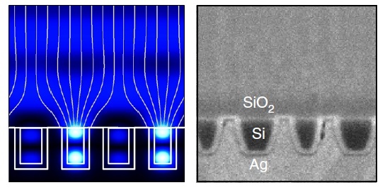
Silicon Mie Resonators for Highly Directional Light Emission from monolayer MoS2 Ahmet Fatih Cihan, Alberto G. Curto, Søren Raza, Pieter G. Kik, Mark L. Brongersma, Nature Photonics 12, 284 (2018) [pdf] [link] Controlling light emission from quantum emitters has important applications, ranging from solid-state lighting and displays to nanoscale single-photon sources. Optical antennas have emerged as promising tools to achieve such control right at the location of the emitter, without the need for bulky, external optics. Semiconductor nanoantennas are particularly practical for this purpose because simple geometries such as wires and spheres support multiple, degenerate optical resonances. Here, we start by modifying Mie scattering theory developed for plane wave illumination to describe scattering of dipole emission. We then use this theory and experiments to demonstrate several pathways to achieve control over the directionality, polarization state and spectral emission that rely on a coherent coupling of an emitting dipole to optical resonances of a silicon nanowire. A forward-to-backward ratio of 20 was demonstrated for the electric dipole emission at 680?nm from a monolayer MoS2 by optically coupling it to a silicon nanowire. Thermoplasmonic Ignition of Metal Nanoparticles Mehmet Mutlu, Ju-Hyung Kang, Søren Raza , David Schoen, Xiaolin Zheng , Pieter G. Kik, and Mark L. Brongersma, Nano Lett. 18, 1699 (2018) [pdf] [link] Explosives, propellants, and pyrotechnics are energetic materials that can store and quickly release tremendous amounts of chemical energy. Aluminum (Al) is a particularly important fuel in many applications because of its high energy density, which can be released in a highly exothermic oxidation process. The diffusive oxidation mechanism (DOM) and melt-dispersion mechanism (MDM) explain the ways powders of Al nanoparticles (NPs) can burn, but little is known about the possible use of plasmonic resonances in NPs to manipulate photoignition. This is complicated by the inhomogeneous nature of powders and very fast heating and burning rates. Here, we generate Al NPs with well-defined sizes, shapes, and spacings by electron beam lithography and demonstrate that their plasmonic resonances can be exploited to heat and ignite them with a laser. By combining simulations with thermal-emission, electron-, and optical-microscopy studies, we reveal how an improved control over NP ignition can be attained. Purcell effect for active tuning of light scattering from semiconductor optical antennas Aaron L. Holsteen, Søren Raza, Pengyu Fan, Pieter G. Kik, and Mark L. Brongersma, Science 358, 1407 (2017) [pdf] [link] Subwavelength, high-refractive index semiconductor nanostructures support optical resonances that endow them with valuable antenna functions. Control over the intrinsic properties, including their complex refractive index, size, and geometry, has been used to manipulate fundamental light absorption, scattering, and emission processes in nanostructured optoelectronic devices. In this study, we harness the electric and magnetic resonances of such antennas to achieve a very strong dependence of the optical properties on the external environment. Specifically, we illustrate how the resonant scattering wavelength of single silicon nanowires is tunable across the entire visible spectrum by simply moving the height of the nanowires above a metallic mirror. We apply this concept by using a nanoelectromechanical platform to demonstrate active tuning. 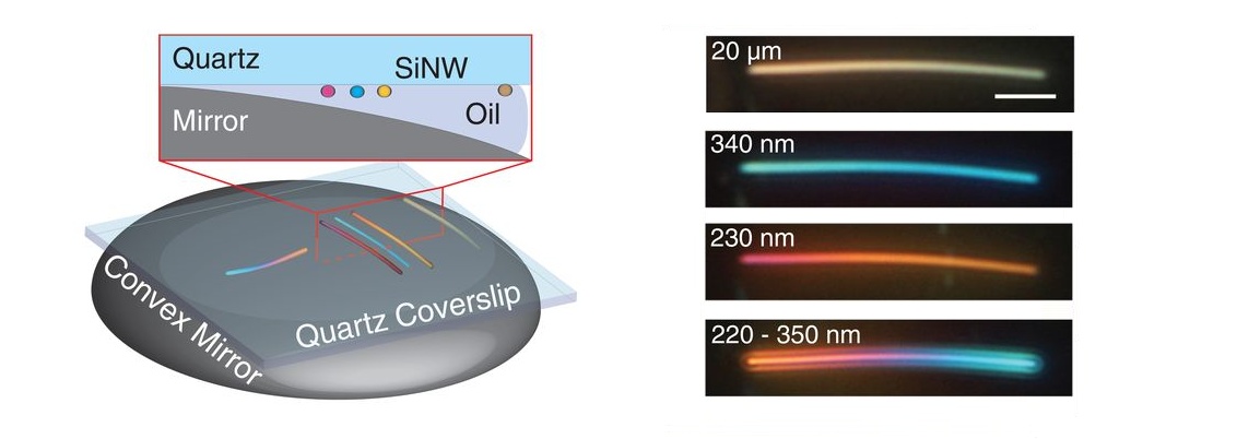
Direct Electrospray Printing of Gradient Refractive Index Chalcogenide Glass Films Spencer Novak, Pao Tai Lin, Cheng Li, Chatdanai Lumdee, Juejun Hu, Anuradha Agarwal, Pieter G. Kik, Weiwei Deng, and Kathleen Richardson, ACS Appl. Mater. Interfaces 9, 26990 (2017) [pdf] [link] A spatially varying effective refractive index gradient using chalcogenide glass layers is printed on a silicon wafer using an optimized electrospray (ES) deposition process. Using solution-derived glass precursors, IR-transparent Ge23Sb7S70 and As40S60 glass films of programmed thickness are fabricated to yield a bilayer structure, resulting in an effective gradient refractive index (GRIN) film. Optical and compositional analysis tools confirm the optical and physical nature of the gradient in the resulting high-optical-quality films, demonstrating the power of direct printing of multimaterial structures compatible with planar photonic fabrication protocols. The potential application of such tailorable materials and structures as they relate to the enhancement of sensitivity in chalcogenide glass based planar chemical sensor device design is presented. This method, applicable to a broad cross section of glass compositions, shows promise in directly depositing GRIN films with tunable refractive index profiles for bulk and planar optical components and devices. Photonic Multitasking Interleaved Si Nanoantenna Phased Array Dianmin Lin, Aaron L. Holsteen, Elhanan Maguid, Gordon Wetzstein, Pieter G. Kik, Erez Hasman, and Mark L. Brongersma, Nano Letters 16, 7671 (2016) [pdf] [link] Metasurfaces provide unprecedented control over light propagation by imparting local, space-variant phase changes on an incident electromagnetic wave. They can improve the performance of conventional optical elements and facilitate the creation of optical components with new functionalities and form factors. Here, we build on knowledge from shared aperture phased array antennas and Si-based gradient metasurfaces to realize various multifunctional metasurfaces capable of achieving multiple distinct functions within a single surface region. As a key point, we demonstrate that interleaving multiple optical elements can be accomplished without reducing the aperture of each subelement. Multifunctional optical elements constructed from Si-based gradient metasurface are realized, including axial and lateral multifocus geometric phase metasurface lenses. We further demonstrate multiwavelength color imaging with a high spatial resolution. Finally, optical imaging functionality with simultaneous color separation has been obtained by using multifunctional metasurfaces, which opens up new opportunities for the field of advanced imaging and display. Superabsorbing, artificial metal films constructed from semiconductor nanoantennas Soo Jin Kim, Junghyun Park, Majid Esfandyarpour, Emanuele Fancesco Pecora, Pieter G. Kik, and Mark L. Brongersma, Nano Lett. 16, 3801 (2016) [pdf] [link] In 1934 Wilhelm Woltersdorff demonstrated that the absorption of light in an ultrathin, freestanding film is fundamentally limited to 50%. He concluded that reaching this limit would require a film with a real-valued sheet resistance that is exactly equal to R=eta/2=188.5 Ohm/sq, where eta = mu0 eps0 is the impedance of free space. This condition can be closely approximated over a wide frequency range in metals that feature a large imaginary relative permittivity eps'', i.e. a real-valued conductivity sigma = eps0 eps'' omega. A thin, continuous sheet of semiconductor material does not facilitate such strong absorption as its complex-valued permittivity with both large real and imaginary components preclude effective impedance matching. In this work, we show how a semiconductor metafilm constructed from optically resonant semiconductor nanostructures can be created whose optical response mimics that of a metallic sheet. For this reason the fundamental absorption limit mentioned above can also be reached with semiconductor materials, opening up new opportunities for the design of ultrathin optoelectronic and light harvesting devices. Omnidirectional excitation of sidewall gap-plasmons in a hybrid goldnanoparticle/aluminum-nanopore structure Chatdanai Lumdee and Pieter G. Kik, APL Photonics 1, 031301 (2016) [pdf] [link] The gap-plasmon resonance of a gold nanoparticle in a nanopore in an aluminum film is investigated in polarization dependent single particle microscopy and spectroscopy. Scattering and transmission measurements reveal that gap-plasmons of this structure can be excited and observed under near-normal incidence excitation and collection, in contrast to the more common particle-on-a-mirror structure. Correlation of numerical simulations with optical spectroscopy suggests that a local electric field enhancement factor in excess of 50 is achieved under normal incidence excitation, with a hot-spot located near the top surface of the structure. It is shown that the strong field enhancement from this sidewall gap-plasmon mode can be efficiently excited over a broad angular range. The presented plasmonic structure lends itself to implementation in low-cost, chemically stable, easily addressable biochemical sensor arrays providing large optical field enhancement factors. Electrospray deposition of uniform thickness Ge23Sb7S70 and As40S60 chalcogenide glass films, Spencer Novak, Pao-Tai Lin, Cheng Li, Nikolay Borodinov, Zhaohong Han, Corentin Monmeyran, Neil Patel, Qingyang Du, Chatdanai Lumdee, Pieter G. Kik, Weiwei Deng, Juejun Hu, Anuradha Agarwal, Igor Luzinov, and Kathleen Richardson, JoVE 54379R3 (2016) Solution-based electrospray film deposition, which is compatible with continuous, roll-to-roll processing, is applied to chalcogenide glasses. Two chalcogenide compositions are demonstrated: Ge23Sb7S70 and As40S60, which have both been studied extensively for planar mid-infrared (mid-IR) microphotonic devices. In this approach, uniform thickness films are fabricated through the use of computer numerical controlled (CNC) motion. Chalcogenide glass (ChG) is written over the substrate by a single nozzle along a serpentine path. Films were subjected to a series of heat treatments between 100 ˚C and 200 ˚C under vacuum to drive off residual solvent and densify the films. Based on transmission Fourier transform infrared (FTIR) spectroscopy and surface roughness measurements, both compositions were found to be suitable for the fabrication of planar devices operating in the mid-IR region. Residual solvent removal was found to be much quicker for the As40S60 film as compared to Ge23Sb7S70. Based on the advantages of electrospray, direct printing of a gradient refractive index Electrically Tunable Coherent Optical Absorption in Graphene with Ion Gel, Vrinda Thareja, Ju-Hyung Kang, Hongtao Yuan, Kaveh M. Milaninia, Harold Y. Hwang, Yi Cui, Pieter G. Kik, and Mark L. Brongersma, Nano Lett. 15, 1570 (2015) [pdf] [link] We demonstrate electrical control over coherent optical absorption in a graphene-based Salisbury screen consisting of a single layer of graphene placed in close proximity to a gold back reflector. The screen was designed to enhance light absorption at a target wavelength of 3.2 µm by using a 600 nm-thick, nonabsorbing silica spacer layer. An ionic gel layer placed on top of the screen was used to electrically gate the charge density in the graphene layer. Spectroscopic reflectance measurements were performed in situ as a function of gate bias. The changes in the reflectance spectra were analyzed using a Fresnel based transfer matrix model in which graphene was treated as an infinitesimally thin sheet with a conductivity given by the Kubo formula. The analysis reveals that a careful choice of the ionic gel layer thickness can lead to optical absorption enhancements of up to 5.5 times for the Salisbury screen compared to a suspended sheet of graphene. In addition to these absorption enhancements, we demonstrate very large electrically induced changes in the optical absorption of graphene of ~3.3% per volt, the highest attained so far in a device that features an atomically thick active layer. This is attributable in part to the more effective gating achieved with the ion gel over the conventional dielectric back gates and partially by achieving a desirable coherent absorption effect linked to the presence of the thin ion gel that boosts the absorption by 40%. Heterogeneous plasmonic trimers for enhanced nonlinear optical absorption, Seyfollah Toroghi, Chatdanai Lumdee, and Pieter G. Kik, Appl. Phys. Lett. 106, 103102 (2015) [pdf] [link] A dramatic enhancement of the thermally induced nonlinear optical response in compositionally heterogeneous plasmonic trimers is reported. It is demonstrated numerically that the nonlinear absorption performance of silver nanoparticle dimers under pulsed illumination can be enhanced by more than two orders of magnitude through the addition of only 0.1 vol.% of gold in the dimer gap. The nonlinear absorption performance of the resulting Ag-Au-Ag trimer exceeds the peak performance of isolated gold nanoparticles by a factor 40. This dramatic effect is enabled by cascaded plasmon resonance, resulting in extreme field concentration in the central nanoparticle of the trimer. The observed localized heat-generation, large optical response, and a predicted response time below 1 ns make these structures promising candidates for use in nonlinear optical limiting and optical switching. Effect of surface roughness on substrate-tuned gold nanoparticle gap plasmon resonances, Chatdanai Lumdee, Binfeng Yun, and Pieter G. Kik, Nanoscale 7, 4250 (2015) [pdf] [link] The effect of nanoscale surface roughness on the gap plasmon resonance of gold nanoparticles on thermally evaporated gold films is investigated experimentally and numerically. Single-particle scattering spectra obtained from 80 nm diameter gold particles on a gold film show significant particle-to-particle variation of the peak scattering wavelength of ±28 nm. The experimental results are compared with numerical simulations of gold nanoparticles positioned on representative rough gold surfaces, modeled based on atomic force microscopy measurements. The predicted spectral variation and average resonance wavelength show good agreement with the measured data. The study shows that nanometer scale surface roughness can significantly affect the performance of gap plasmon-based devices. Gap-Plasmon Enhanced Gold Nanoparticle Photoluminescence, Chatdanai Lumdee, Binfeng Yun, and Pieter G. Kik, ACS Photonics 1, 1224 (2014) [pdf] [link] [cover] [supporting info] Gap-plasmon enhanced gold nanoparticle photoluminescence is studied experimentally at the single particle level. The photoluminescence spectra of gold nanoparticles on an Al2O3-coated gold film under both 532 nm and 633 nm excitation show a clear peak near the measured gap plasmon resonance wavelength. Comparing the collected emission spectrum with that from a gold reference film under 633 nm excitation, a peak photoluminescence enhancement factor of 28000 is observed. The spectral shape and absolute magnitude of the enhancement factors for both excitation wavelengths are reproduced using numerical calculations without the use of any free parameters. The photoluminescence enhancement is explained in terms of a gap-mode enhanced e-h pair generation rate and a wavelength-dependent enhancement of the emission efficiency. Related publications: 2013: Wide-band Spectral Control of Au Nanoparticle Plasmon Resonances pdf / link 2012: Voltage Controlled Resonance Tuning of Nanoscale Plasmonic Antennas pdf / link 2010: Metal-film-induced tuning of silver nanoparticle plasmon resonances pdf / link 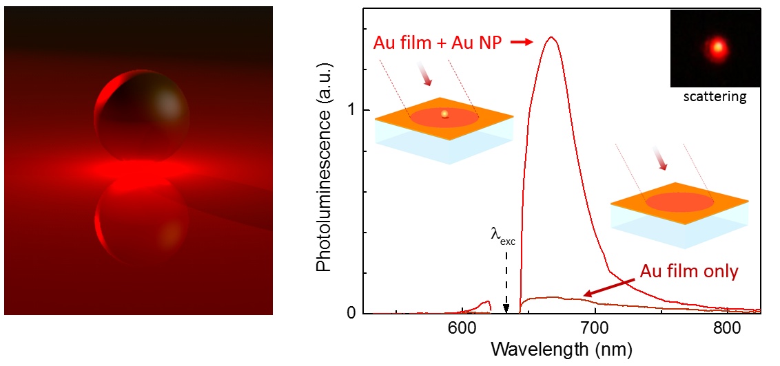
Photothermal response enhancement in heterogeneous plasmon resonant nanoparticle trimers, Seyfollah Toroghi and Pieter G. Kik, Phys. Rev. B 90, 205414 (2014) [pdf] [link] The optical response of heterogeneous plasmonic trimer structures composed of a silver nanoparticle dimer and a central gold nanoparticle is investigated analytically and numerically. The plasmon resonance of the silver dimer is controlled through near-field coupling, resulting in plasmon resonance frequency matching of the silver dimer and gold monomer. This coupling condition makes it possible to increase the energy dissipation per unit volume in the gold particle by over two orders of magnitude compared to a single-particle system. It is predicted that pulsed illumination of a trimer consisting of two 80 nm diameter silver particles and a 10 nm diameter central gold particle can raise the gold particle temperature by 100 K using a pump fluence as low as 20 nJ/mm2 at a wavelength of 530 nm. This finding may have practical applications in photothermal therapy, fast thermal nonlinear optical modulation, and could enable new fundamental thermal studies at picosecond time scales. 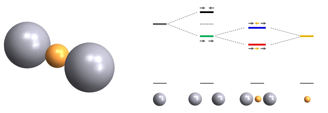
Catoptric electrodes: transparent metal electrodes using shaped surfaces, Pieter G. Kik, Opt. Lett. 39, 5114 (2014) [pdf] [link] An optical electrode design is presented that theoretically allows 100% optical transmission through an interdigitated metallic electrode at 50% metal areal coverage. This is achieved by redirection of light incident on embedded metal electrode lines to an angle beyond that required for total internal reflection. Full-field electromagnetic simulations using realistic material parameters demonstrate 84% frequency-averaged transmission for unpolarized illumination across the entire visible spectral range using a silver interdigitated electrode at 50% areal coverage. The redirection is achieved through specular reflection, making it non-resonant and arbitrarily broadband, provided the electrode width exceeds the optical wavelength. These findings could significantly improve the performance of photovoltaic devices and optical detectors that require high-conductivity top contacts. 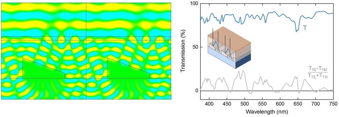
Numerical prediction of the effect of nanoscale surface roughness on film-coupled nanoparticle plasmon resonances, C. Lumdee and P. G. Kik, Proc. SPIE 9163, 91631I (2014) [pdf] [link] Plasmon-enhanced photothermal response in heterogeneous metallic trimers, S. Toroghi and P. G. Kik, Proc. SPIE 9163, 91631B (2014) [pdf] [link] Wide-band Spectral Control of Au Nanoparticle Plasmon Resonances on a Thermally and Chemically Robust Sensing Platform, Chatdanai Lumdee, Binfeng Yun, and Pieter G. Kik, J. Phys. Chem. C 117, 19127 (2013) [pdf] [link] Gold nanoparticles on Al2O3-coated gold films are presented as a chemically and thermally robust platform for molecular sensing. Single particle spectroscopy as a function of Al2O3 coating thickness shows reproducible gold nanoparticle scattering spectra in the range from 690 nm to 610 nm as the Al2O3 thickness increases from 0 to 3.4 nm. Numerical simulation of these structures indicates that surface enhanced Raman spectroscopy enhancement factors in excess of 10^6 can be achieved. The stability of the Al2O3 coated structures under high power laser irradiation was tested, revealing stable scattering spectra upon irradiation with 100 W/mm2 at the particle resonance wavelength. The presented structure solves challenges with thermal stability, wavelength tuning range, and Raman background signal associated with previously attempted approaches. 
Cascaded plasmon resonances in multi-material nanoparticle trimers for extreme field enhancement, S. Toroghi, C. Lumdee, and P. G. Kik, Proc. SPIE 8809, 88091M (2013) [pdf] [link] Optical Characteristics and Numerical Study of Gold Nanoparticles on Al2O3 coated Gold Film for Tunable Plasmonic Sensing Platforms, C. Lumdee, B. Yun, and P. G. Kik, Proc. SPIE 8809, 88091S (2013) [pdf] [link] Controlled Surface Plasmon Resonance on Stable Substrates as an Optimized Sensing Platform, C. Lumdee, B. Yun, and P. G. Kik, Paper FTh3C.8, Frontiers in Optics Conference (2013) [pdf] [link] Extreme plasmon resonant field enhancement in multi-material nanoparticle trimers, Seyfollah Toroghi, Chatdanai Lumdee, and Pieter G. Kik, Paper FTh3C.3, Frontiers in Optics Conference (2013) [pdf] [link] Post-Fabrication Voltage Controlled Resonance Tuning of Nanoscale Plasmonic Antennas, Chatdanai Lumdee, Seyfollah Toroghi, and Pieter G. Kik, ACS Nano 6, 6301 (2012) [pdf] [link] Voltage controlled wavelength tuning of the localized surface plasmon resonance of gold nanoparticles on an aluminum film is demonstrated in single particle microscopy and spectroscopy measurements. Anodization of the Al film after nanoparticle deposition forms an aluminum oxide spacer layer between the gold particles and the Al film, modifying the particle-substrate interaction. Darkfield microscopy reveals ring-shaped scattering images from individual Au nanoparticles, indicative of plasmon resonances with a dipole moment normal to the substrate. Single particle scattering spectra show narrow plasmon resonances that can be tuned from ~580 nm to ~550 nm as the anodization voltage increases to 12 V. All observed experimental trends could be reproduced in numerical simulations. The presented approach could be used as a general post-fabrication resonance optimization step of plasmonic nanoantennas and devices. 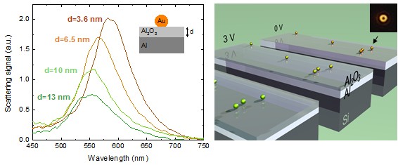
Cascaded field enhancement in plasmon resonant dimer nanoantennas compatible with two-dimensional nanofabrication methods, Seyfollah Toroghi and Pieter G. Kik, Appl. Phys. Lett. 101, 13116 (2012) [pdf] [link] Cascaded field enhancement is demonstrated in asymmetric plasmon resonant dimer nanoantennas consisting of shape-tuned ellipsoidal nanoparticles. The nanoparticles that make up the dimer have identical thickness, suggesting that the presented approach can be used to design cascaded dimer antennas compatible with standard two-dimensional top-down nanofabrication tools such as electron beam lithography and nano-imprint lithography. Cascaded excitation is achieved by modification of the in-plane particle aspect ratios in a way that keeps the resonance frequency of the individual particles fixed, while significantly changing their polarizability. The achievable field enhancement is evaluated as a function of the particle volume ratio and spacing. 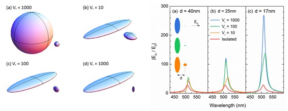
Cascaded plasmon resonant field enhancement in nanoparticle dimers in the point dipole limit, Seyfollah Toroghi and Pieter G. Kik, Appl. Phys. Lett. 100, 183105 (2012) [pdf] [link] Cascaded field enhancement in silver dimer nanostructures is investigated using a dipole-dipole interaction model. Field enhancement spectra are evaluated as a function of the particle size difference and inter-particle spacing. We observe three distinct regimes of cascaded field enhancement: hindered cascading, multiplicative cascading, and the ultimate cascading limit, depending on the dimer interaction strength. Multiplicative cascading at small inter-particle spacing leads to analytic expressions for the ultimate internal and external field enhancement factors. For silver dimers in a host with index 1.5 we obtain a maximum internal field enhancement of 2.9E3, a factor of 75 larger than that of an isolated silver nanoparticle. 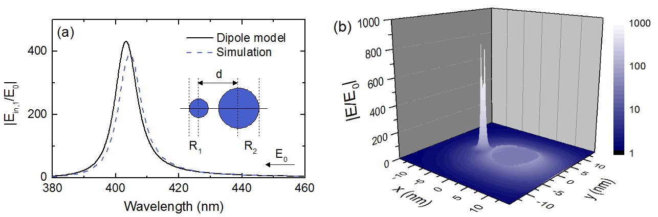
Cascaded plasmonic metamaterials for phase-controlled enhancement of nonlinear absorption and refraction, Seyfollah Toroghi and Pieter G. Kik, Phys. Rev. B 85, 045432 (2012) [pdf] [link] The nonlinear optical properties of plasmon resonant metamaterials consisting of chains of metal nanoparticles are evaluated. Introducing particle size differences along the chains leads to the development of cascaded plasmon resonances exhibiting increased field enhancement and field confinement. The interplay between the different resonances on the structures induces a frequency dependent enhancement of the nonlinear refractive and absorptive response of the metamaterial, ultimately providing larger nonlinear susceptibility enhancement factors with engineered complex phase. It is shown that cascaded structures can provide a figure of merit for nonlinear absorption that is more than an order of magnitude larger than that obtained in non-cascaded structures. The presented approach could lead to new planar and integrated nonlinear optical modulation and switching media with improved performance compared to their non-cascaded counterparts. 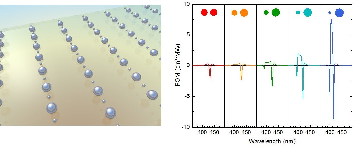
Taking cascaded plasmonic field enhancement to the ultimate limit in silver nanoparticle dimers, Seyfollah Toroghi and Pieter G. Kik, Proc. SPIE 8457, 84570D (2012) [pdf] [link] Cascaded optical field enhancement in coupled plasmonic nanostructures has attracted significant attention because of field enhancement factors that dramatically exceed those observed in isolated nanostructures. While previous studies demonstrated the existence of cascaded enhancement, little work has been done to identify the requirements for achieving maximum field enhancement. Here, we investigate cascaded field enhancement in silver nanosphere dimers as a function of volume ratio and center-to-center separation, and show the requirements for achieving the ultimate cascading limit in nanoparticle dimers. We observe field enhancements that are a factor 75 larger than observed in isolated silver nanoparticles. Voltage controlled nanoparticle plasmon resonance tuning through anodization, Chatdanai Lumdee and Pieter G. Kik, Proc. SPIE 8457, 84570T (2012) [pdf] [link] Frequency control of plasmon resonances is important for optical sensing applications such as Surface Enhanced Raman Spectroscopy. Prior studies that investigated substrate-based control of noble metal nanoparticle plasmon resonances mostly relied on metal substrates with organic or oxide spacer layers that provided a fixed resonance frequency after particle deposition. Here we present a new approach enabling continuous resonance tuning through controlled substrate anodization. Localized Surface Plasmon tuning of single gold nanoparticles on an Al film is observed in single-particle microscopy and spectroscopy experiments. Au nanoparticles (diameter 60 nm) are deposited on 100 nm thick Al films on silicon. Dark field microscopy reveals Au nanoparticles with a dipole moment perpendicular to the aluminum surface. Subsequently an Al2O3 film is formed with voltage controlled thickness through anodization of the particle coated sample. Spectroscopy on the same particles before and after various anodization steps reveal a consistent blue shift as the oxide thickness is increased. The observed trends in the scattering peak position are explained as a voltage controlled interaction between the nanoparticles and the substrate. The experimental findings are found to closely match numerical simulations. The effects of particle size variation and spacer layer dielectric functions are investigated numerically. The presented approach could provide a post-fabrication frequency tuning step in a wide range of plasmonic devices, could enable the investigation of the optical response of metal nanostructures in a precisely controlled local environment, and could form the basis of chemically stable frequency optimized sensors. Design of cascaded plasmon resonances for ultrafast nonlinear optical switching, Seyfollah Toroghi and Pieter G. Kik, SPIE 8054, 80540E-1 (2011) [pdf] [link] The optical properties of cascaded plasmon resonant metallic nanocomposites are investigated. Plasmon resonances and their related field distributions are numerically evaluated in two-dimensional arrays of spherical silver nanoparticles embedded in a dielectric host. The field distributions in structures with identical particle sizes indicate the presence of a largely dipolar particle response, with a small multipole resonance contribution at high frequency. However, in arrays consisting of particles with dissimilar sizes, an additional coupled mode appears in which the dipole moment in adjacent particles is found to be anti-parallel. For increasing size-dissimilarity a higher electric field enhancement is observed inside the small metal nanospheres, indicative of a cascaded field enhancement effect. This effect may be used to enhance the nonlinear optical response of an effective medium composed of particles with engineered size dispersion and particle placement. 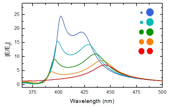
Determination of optimum Si excess concentration in Er-doped Si-rich SiO2 for optical amplification at 1.54 um , Oleksandr Savchyn, Kevin R. Coffey, and Pieter G. Kik, Appl. Phys. Lett. 97, 201107 (2010) [pdf] [link] The presence of indirect Er3+ excitation in Si-rich SiO2 is demonstrated for Si excess concentrations in the range 2.5 – 37 at.%. The Si excess concentration providing the highest density of sensitized Er3+ ions is demonstrated to be relatively insensitive to the presence of Si nanocrystals and is found to be ~ 14.5 at.% for samples without Si nanocrystals (annealed at 600°C) and ~ 11.5 at.% for samples with Si nanocrystals (annealed at 1100°C). The observed optimum is attributed to an increase in the density of Si-related sensitizers as the Si concentration is increased, with subsequent deactivation and removal of these sensitizers at high Si concentrations. The optimized Si excess concentration is predicted to generate maximum Er-related gain at 1.54 μm in devices based on Er-doped Si-rich SiO2. Frequency dependent power efficiency of a nanostructured surface plasmon coupler, Amitabh Ghoshal and Pieter G. Kik, Phys. Stat. Sol. Rapid Research Letters 4, 280 (2010) [pdf] [link] [cover] [cover info] Surface plasmon (SP) excitation on an extended thin metal film via a miniature nanoparticle-enhanced grating coupler is studied experimentally using leakage radiation spectroscopy. A universally applicable method for determining the efficiency of free-space SP excitation is developed, and the efficiency of the coupler is determined. Two distinct grating excitation modes are observed, as well as a particle-mediated excitation mode. The maximum observed coupling efficiency of the structure was approximately 3.5% at 615 nm and 670 nm, corresponding to the two grating modes of the structure. 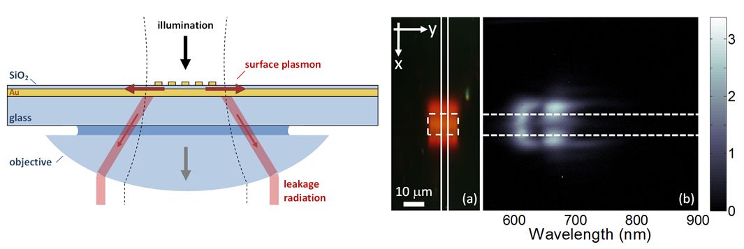
Single particle spectroscopy study of metal-film-induced tuning of silver nanoparticle plasmon resonances, Min Hu, Amitabh Ghoshal, Manuel Marquez, and Pieter G. Kik, J. Phys. Chem. C 114, 7509 (2010) [pdf] [link] We present an experimental study of the tunability of the silver nanoparticle localized plasmon resonance in close proximity to a gold film. Broadband tuning of the silver particle plasmon resonance from blue wavelengths into the near-IR region can be achieved due to strong electromagnetic coupling between the nanoparticle and the metal film. By altering the thickness of a thin silica spacer layer between the metal nanoparticle and the metal film the resonance frequency can be selected. Single particle spectroscopy of over 250 isolated silver nanoparticles revealed evidence for the excitation of both horizontal and vertical plasmon modes. Distinct resonance features observed in the scattering spectra were assigned to specific modes based on a dipole-dipole interaction model. The experimental results suggest that low-loss silver nanoparticles can be used in surface enhanced spectroscopy studies throughout the entire visible spectrum. The use of frequency tuned spherical metal nanoparticles on solid substrates could lead to thermally stable substrates for plasmon enhanced sensing applications, including surface enhanced Raman scattering and refractive index based biodetection methods. 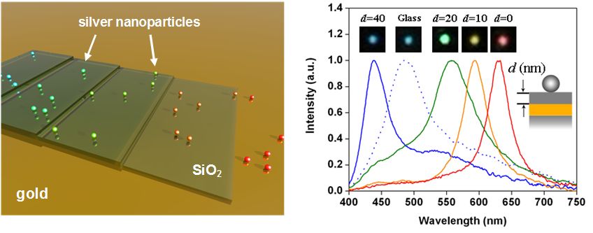
High temperature optical properties of sensitized Er3+ in Si-rich SiO2 - implications for gain performance , Oleksandr Savchyn, Ravi M. Todi, Kevin R. Coffey, and Pieter G. Kik, Opt. Mat. 32, 1274 (2010) [pdf] [link] The high-temperature photoluminescence of Er-doped Si-rich SiO2 with and without silicon nanocrystals is studied at sample temperatures in the range 20 – 200oC. The optical properties of Er-doped Si-rich SiO2 with and without silicon nanocrystals are shown to exhibit a similar temperature dependence. Based on the measured photoluminescence intensities and lifetimes it is predicted that an increase of the sample temperature from 20°C to 200oC results in a decrease of the maximum optical gain at 1535 nm by a factor of ~ 1.8 and ~ 1.6 for samples with and without nanocrystals respectively. Implementation of this material in silicon photonics requires stable operation at typical processor case temperatures up to 80 – 90oC. It is demonstrated that increasing the temperature from room temperature to 90°C leads to a predicted maximum optical gain reduction of ~ 1.26 for both materials. In addition, the predicted erbium related optical gain at significant inversion levels in samples processed at low temperature (600°C) is a factor ~ 9 higher than for samples processed at high temperature (1060°C). These findings demonstrate that relatively thermally stable gain performance of the Er-doped Si-rich SiO2 up to typical processor operating temperatures is possible and indicate that low-temperature-processed erbium-doped silicon-rich SiO2 is a technologically viable gain medium for use in silicon photonics. Near-field enhancement of infrared intensities for f-f transitions in Er3+ ions close to the surface of silicon nanoparticles, Lesya Borowska, Stephan Fritzsche, Pieter G. Kik, and Artem E. Masunov, J. Mol. Model. 17, 423 (2010) [pdf] [link] Erbium doped waveguide amplifiers can be used in optical integrated circuits to compensate for signal losses. Such amplifiers use stimulated emission from the first excited state (4I13/2) to the ground state (4I15/2) of Er3+ at 1.53 μm, the standard wavelength for optical communication. Since the intra-f transitions are parity forbidden for free Er3+ ions, the absorption and the emission cross sections are quite small for such doped amplifiers. To enhance the absorption, Si nanoclusters can be embedded in silica matrix. Here we investigate the effect of the Si nanocluster on the Er emission using ab initio theory for the first time. We combine multi-reference configuration interaction with one-electron spin-orbit Hamiltonian and relativistic effective core potentials. Our calculations show that the presence of a polarizable Be atom at 5A from the Er3+ ion in a crystalline environment can lead to an enhancement in the emission by a factor of three. The implications of this effect in designing more efficient optical gain materials are discussed. Excitation wavelength-independent sensitized Er3+ concentration in as-deposited and low temperature annealed Si-rich SiO2 films, Oleksandr Savchyn, Ravi M. Todi, Kevin R. Coffey, Luis K. Ono, Beatriz Roldan Cuenya, and Pieter G. Kik, Appl. Phys. Lett. 95, 231109 (2009) [pdf] [link] Erbium sensitization is observed in as-deposited Er3+ doped Si-rich SiO2, ruling out the involvement of Si nanocrystals in the Er3+ excitation in these samples. The Er3+ absorption cross section in this material is similar within a factor 3 to that of samples annealed at 600oC under 355nm and 532nm excitation. The density of excitable Er3+ ions is shown to be excitation wavelength independent, while the shape of the Er3+ excitation spectra is governed by a wavelength-dependent Er3+ absorption cross section. These findings enable the use of a broad range of wavelengths for the efficient excitation of this gain medium. Structural control of nonlinear optical absorption and refraction in dense metal nanoparticle arrays, Dana C. Kohlgraf-Owens and Pieter G. Kik, Opt. Express 17, 15032 (2009) [pdf] [link] The linear and nonlinear optical properties of a composite containing interacting spherical silver nanoparticles embedded in a dielectric host are studied as a function of interparticle separation using three dimensional frequency domain simulations. It is shown that for a fixed amount of metal, the effective third-order nonlinear susceptibility of the composite X(3) can be significantly enhanced with respect to the linear optical properties, due to a combination of resonant surface plasmon excitation and local field redistribution. It is shown that this geometry-dependent susceptibility enhancement can lead to an improved figure of merit for nonlinear absorption. Enhancement factors for the nonlinear susceptibility of the composite are calculated, and the complex nature of the enhancement factors is discussed. 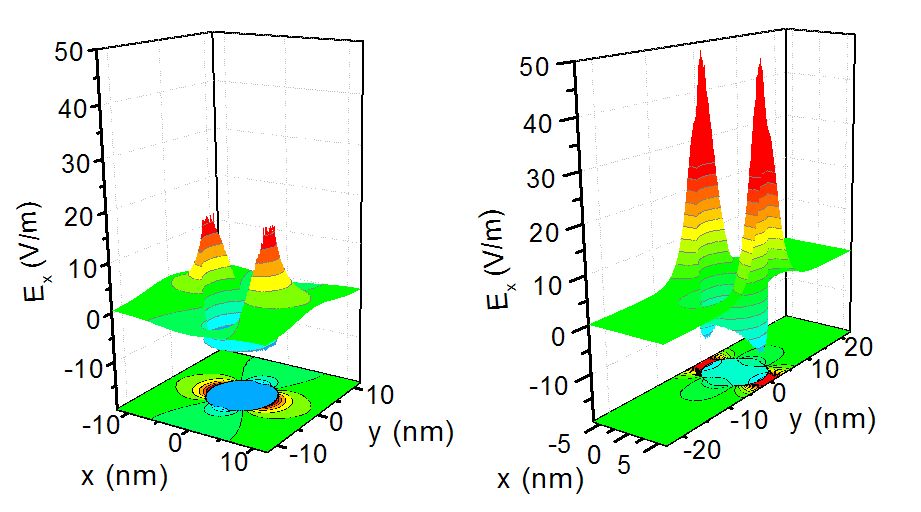
Observation of temperature-independent internal Er3+ relaxation efficiency in Si-rich SiO2 films, Oleksandr Savchyn, Ravi M. Todi, Kevin R. Coffey, and Pieter G. Kik, Appl. Phys. Lett. 94, 241115 (2009) [pdf] [link] Time-dependent photoluminescence measurements of low-temperature-annealed Er-doped Si-rich SiO2 were conducted at sample temperatures 15-300K. The erbium internal relaxation efficiency from the second (4I11/2) to the first (4I13/2) excited state upon luminescence-center-mediated Er3+ excitation is investigated. Despite the observation of temperature-dependent relaxation rates, the erbium internal relaxation efficiency is found to be remarkably temperature-independent, which suggests that the internal relaxation efficiency is near-unity. Internal relaxation is shown to account for 50-55% of the 4I13/2 excitation events in the entire temperature range. These results demonstrate that high pump efficiency and stable operation of devices based on this material will be possible under varying thermal conditions. Excitation of propagating surface plasmons by a periodic nanoparticle array: trade-off between particle-induced near-field excitation and damping, Amitabh Ghoshal and Pieter G. Kik, Appl. Phys. Lett. 94, 251102 (2009) [pdf] [link] The excitation of propagating surface plasmons (SPs) on a silver-SiO2 interface by an array of ellipsoidal silver nanoparticles is investigated using numerical simulations as a function of particle volume for three different nanoparticle aspect ratios. We find that while the SP amplitude depends sensitively on particle volume for each selected aspect ratio, the maximum SP amplitude obtained for the different particle shapes is remarkably similar. These observations are explained in terms of particle-mediated SP excitation, counteracted by a size dependent particle-induced damping. An analytical model is presented that quantitatively describes the observed trends in SP damping. Experimental observation of mode-selective anticrossing in surface-plasmon-coupled metal nanoparticle arrays, Amitabh Ghoshal, Ivan Divliansky, and Pieter G. Kik, Appl. Phys. Lett. 94, 171108 (2009) [pdf] [link] Surface plasmon excitation using resonant metal nanoparticles is studied experimentally. Geometry dependent reflection measurements reveal the existence of several optical resonances. Strong coupling of the in-plane nanoparticle plasmon resonance and propagating plasmons is evident from clear anticrossing behavior. Reflection measurements at high numerical aperture demonstrate the excitation of surface plasmons via out-of-plane particle polarization. The thus excited plasmons do not exhibit anticrossing in the considered frequency range. The results are explained in terms of the known surface plasmon dispersion relation and the anisotropic frequency dependent nanoparticle polarizability. These findings are important for applications utilizing surface-coupled nanoparticle plasmon resonances. Multi-level sensitization of Er3+ in low-temperature-annealed silicon-rich SiO2, Oleksandr Savchyn, Ravi M. Todi, Kevin R. Coffey, and Pieter G. Kik, Appl. Phys. Lett. 93, 233120 (2008) [pdf] [link] Linear and Nonlinear Effective Medium Properties of Metallodielectric Composites of Interacting Spheres and Isolated Spheroids, Dana C. Kohlgraf-Owens and Pieter G. Kik, in Plasmonics and Metamaterials, OSA Technical Digest, paper MThB3 (2008) [pdf] [link] Numerical study of surface plasmon enhanced nonlinear absorption and refraction, Dana C. Kohlgraf-Owens and Pieter G. Kik, Optics Express 16, 16823 (2008) [pdf] [link] Effect of hydrogen passivation on luminescence-center-mediated Er excitation in Si rich SiO2 with and without Si nanocrystals, Oleksandr Savchyn, Pieter G. Kik, Ravi M. Todi, and Kevin R. Coffey, Phys. Rev. B 77, 205438 (2008) [pdf] [link] Simultaneous excitation of fast and slow surface plasmon polaritons in a high dielectric contrast system, Grady Webb-Wood and Pieter G. Kik, Appl. Phys. Lett. 92, 133101 (2008) [pdf] [link] Theory and simulation of surface plasmon excitation using resonant metal nanoparticle arrays, Amitabh Ghoshal and Pieter G. Kik, J. Appl. Phys. 103, 113111 (2008) [pdf] [link] Surface Plasmon Nanophotonics, Mark L. Brongersma and Pieter G. Kik (Eds.), Springer Series in Optical Sciences (2007) [chapter 1] [book website] 
Luminescence center mediated excitation as the dominant erbium sensitization mechanism in Er-doped silicon-rich SiO2 films, Oleksandr Savchyn, Forrest R. Ruhge, Pieter G. Kik, Ravi M. Todi, Kevin R. Coffey, Haritha Nukala, and Helge Heinrich, Phys. Rev. B 76, 195419 (2007) [pdf] [link] Optimization of surface plasmon excitation using resonant nanoparticle arrays above a silver film, Amitabh Ghoshal and Pieter G. Kik, Proc. SPIE 6641, 664119 (2007) [pdf] [link] Demonstration of three dimensional imaging of blood vessel using a no moving parts electronic lens-based optical confocal microscope, Nabeel A. Riza, Mumtaz Sheikh, Grady Webb-Wood, and Pieter Kik, Proc. SPIE 6510, 65100J (2007) [pdf] [link] Optical and morphological properties of MBE grown wurtzite CdxZn1-xO thin films, J.W. Mares, F.R. Ruhge, A.V. Thompson, P.G. Kik, A. Osinsky, B. Hertog, A.M. Dabiran, P.P. Chow, and W.V. Schoenfeld, Opt. Mater. 30, 346 (2007) [pdf] [link] In-situ experimental study of a near-field lens at visible frequencies, Grady Webb-Wood, Amitabh Ghoshal, and Pieter G. Kik, Appl. Phys. Lett. 89, 193110 (2006) [pdf] [link] Coherent far-field excitation of surface plasmons using resonantly tuned metal nanoparticle arrays, Amitabh Ghoshal, Grady Webb-Wood, Clarisse Mazuir, and Pieter G. Kik, Proc. SPIE 5927, 592714 (2005) [pdf] [link] Silicon optical nanocrystal memory, R.J. Walters, P.G. Kik, J.D. Casperson, H.A. Atwater, R. Lindstedt, M. Giorgi, and G. Bourianoff, Appl. Phys. Lett. 85, 2622 (2004) [pdf] Image resolution of surface-plasmon-mediated near-field focusing with planar metal films in three dimensions using finite-linewidth dipole sources, P.G. Kik, S.A. Maier, and H.A. Atwater, Phys. Rev. B 69, 45418 (2004) [pdf] [link] Optical pulse propagation in metal nanoparticle chain waveguides, S.A. Maier, P.G. Kik, and H.A. Atwater, Phys. Rev. B 67, 205402 (2003) [pdf] Local detection of electromagnetic energy transport below the diffraction limit in metal nanoparticle plasmon waveguides, S.A. Maier, P.G. Kik, H.A. Atwater, S. Meltzer, E. Harel, B.E. Koel, A.A.G. Requicha, Nature Materials 2, 229-232 (2003) [pdf] Cooperative upconversion as the gain-limiting factor in Er doped miniature Al2O3 optical waveguide amplifiers, P.G. Kik and A. Polman, J. Appl. Phys. 93, 5008 (2003) [pdf] [link] Towards an Er-doped Si nanocrystal sensitized waveguide laser, P.G. Kik, and A.Polman, Proceedings NATO Workshop OASIS (2002) [pdf] Metal nanoparticle arrays for near field optical lithography, P.G. Kik, S.A. Maier, and H.A. Atwater, SPIE Proceedings (2002) [pdf] Observation of coupled plasmon-polariton modes in Au nanoparticle chain waveguides of different lengths: Estimation of waveguide loss, S. A. Maier, P. G. Kik, and H. A. Atwater, Appl. Phys. Lett. 81, 1714 (2002) [pdf] Observation of near-field coupling in metal nanoparticle chains using far-field polarization spectroscopy, S. A. Maier, M. L. Brongersma, P. G. Kik, and H. A. Atwater, Phys. Rev. B 65, 193408 (2002) [pdf] Plasmon printing - a new approach to near-field lithography, P.G. Kik, S.A. Maier, and H.A. Atwater, Mat. Res. Soc. Symp. Proc. 705, Y3.6 (2002) [pdf] Design and Performance of an Erbium-Doped Silicon Waveguide Detector Operating at 1.5 um, P. G. Kik, A. Polman, S. Libertino, and S. Coffa, J. Lightwave Technol. 20, 862 (2002) [pdf] Gain limiting processes in Er-doped Si nanocrystal waveguides in SiO2, P. G. Kik and A. Polman, J. Appl. Phys. 91, 534 (2002) [pdf] [link] Plasmonics - A route to nanoscale optical devices, S.A. Maier, M.L. Brongersma, P.G. Kik, S. Meltzer, A.A.G. Requicha, and H.A. Atwater, Adv. Mater. 13, 1501 (2001) [pdf] Pumping planar waveguide amplifiers using a coupled waveguide system, L.H. Slooff, P.G. Kik, A. Tip, A. Polman, J. Lightwave Technol. 19, 1740 (2001) [pdf] Exciton-erbium energy transfer in Si nanocrystal-doped SiO2, P.G. Kik, and A. Polman, Mat. Sc. Eng. B 81, 3 (2001) [pdf] Energy transfer in erbium doped optical waveguides based on silicon, P.G. Kik, Ph.D. Thesis, Utrecht University, The Netherlands (2000) [pdf] Energy backtransfer and infrared photoresponse in erbium doped silicon p-n diodes, N. Hamelin, P.G. Kik, and A. Polman, J. Appl. Phys. 88, 5381 (2000) [pdf] Selective modification of the Er3+ 4I11/2 branching ratio by energy transfer to Eu3+, C. Strohhöfer, P.G. Kik, and A. Polman, J. Appl. Phys. 88, 4486 (2000) [pdf] Exciton-erbium interactions in Si nanocrystal-doped SiO2, P.G. Kik and A. Polman, J. Appl. Phys. 88, 1992 (2000) [pdf] [link] Strong exciton-erbium coupling in Si nanocrystal-doped SiO2, P.G. Kik, M.L. Brongersma, A. Polman, Appl. Phys. Lett. 76, 2325 (2000) [pdf] Size-dependent electron-hole exchange interaction in Si nanocrystals, M.L. Brongersma, P.G. Kik, A. Polman, K.S. Min. and H.A. Atwater, Appl. Phys. Lett. 76, 351 (2000) [pdf] Optical and electrical doping of silicon with holmium, J.F. Suyver, P.G. Kik, T. Kimura, A. Polman, G. Franzò, S. Coffa, Nucl. Instrum. Meth. B 148, 497 (1999) [pdf] Erbium doped optical-waveguide amplifiers on silicon, P.G. Kik, A. Polman, Mat. Res. Soc. Bull. 23, 48 (1998) [pdf] [link] Erbium-doped phosphate glass waveguide on silicon with 4.1 dB/cm gain at 1.535 mm, Y.C. Yan, A.J. Faber, H. de Waal, P.G. Kik, and A. Polman, Appl. Phys. Lett. 71, 2922 (1997) [pdf] Excitation and de-excitation of Er3+ in crystalline silicon, P.G. Kik, M.J.A. de Dood, K. Kikoin, and A. Polman, Appl. Phys. Lett. 70, 1721 (1997) [pdf] Incorporation, excitation, and de-excitation of erbium in crystal silicon, M.J.A. de Dood, P.G. Kik, J.H. Shin, and A. Polman, Mat. Res. Soc. Symp. Proc. 422, 219 (1996) Concentration quenching in erbium implanted alkali silicate glasses, E. Snoeks, P.G. Kik, A. Polman, Opt. Mater. 5, 159 (1996) [pdf] Ion beam synthesis of planar opto-electronic devices, A. Polman, E. Snoeks, G.N. van den Hoven, M.L. Brongersma, R. Serna, J.H. Shin, P.G. Kik, E. Radius, Nucl. Instrum. Meth. B 106, 393 (1995) [pdf] |