| > Kik Group | College of Optics and Photonics | UCF |
|
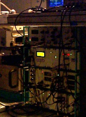
CREOL Nanophotonics Fabrication Facility The College of Optics and Photonics houses two main cleanrooms, the largest of which is located on the ground floor. This cleanroom, called the Nanophotonics Fabrication Facility, covers an area of 3000 sqft including a 1500 sqft Class 100 section. This means that a cubic foot of cleanroom air contains fewer than 100 dust particles larger than 0.0005 mm, which is necessary to fabricate defect-free nanoscale photonic structures. This gallery shows examples of tools in the accessible to students in the Kik group that allow us to design and characterize nanophotonic circuits with sub-100nm dimensions.

Leica EBPG 5000+ Electron Beam Lithography system This shows the EBL system, located in the class 100 section of the cleanroom. The EBPG 5000+ allows us to use an electron beam with energies up to 100keV to write patterns in electron beam resist with a resolution better than 50nm across a 0.5mm x0.5mm area. Metal deposition onto the developed resist and subsequent liftoff enables the formation of metal nanophotonic integrated circuits. |