| > Kik Group | College of Optics and Photonics | UCF |
|
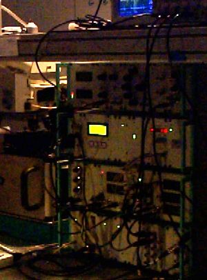
Laboratory The study of nanophotonic structures requires an array of dedicated equipment, including various light sources, detectors, electronics, nanopositioning equipment, software, and more. This section shows the main tools in use in our NanoPhotonics Characterization Lab. Students in the group actively fabricate nanophotonic structures using CREOL's own NanoPhotonics Fabrication Facility. For an impression of the tools that the group uses, have a look at the cleanroom photo gallery. Witec Near-field Scanning Optical Microscope 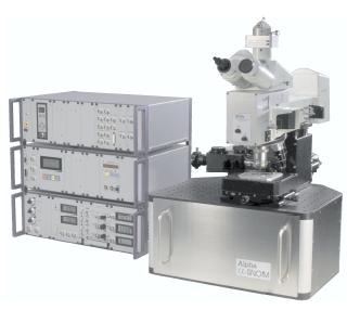
A core component of the NanoPhotonics Characterization lab is the
Witec AlphaSNOM,
a combined Near-field Scanning Optical Microscope (NSOM), Atomic Force Microscope (AFM), and Confocal Microscope.
All three techniques are indispensable in the investigation of nanophotonic structures. Woollam M2000 Spectroscopic Ellipsometer 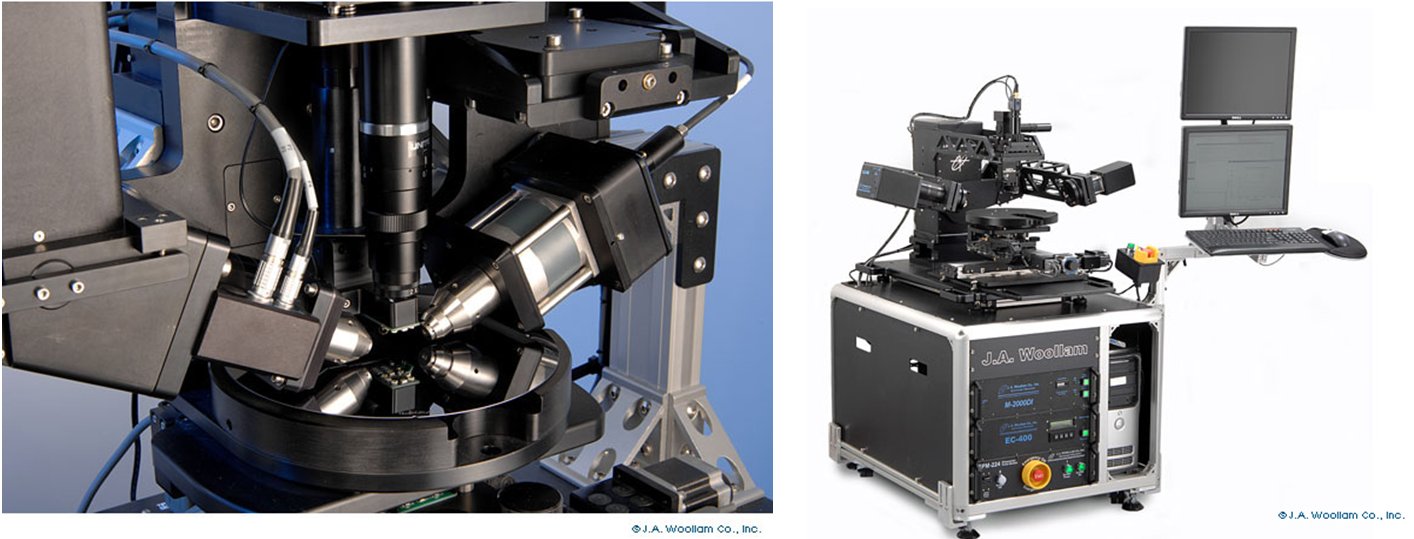
The M2000
High-Speed Scanning Variable Angle Spectroscopic Ellipsometer is a thin film and multilayer analysis tool that enables the
rapid determination of linear optical properties (refractive index, absorption coefficient, depolarization factors, anisotropy) in a wide
wavelength range spanning the UV, VIS, and NIR. The system, manufactured by
J. A. Woollam
is equipped with custom focusing optics that enable a measurement spot size as small as 100x100 um2.
Array based detectors enable data collection across the full spectral range in under 5 seconds.
The system features automated mapping, useful for example for the detection of film thickness gradients, semiconductor bandgap variation across a deposited layer,
thickness homogeneity of a planar waveguide, etc. For more information, see the M2000 system specifications
and a list of sample requirements. |