|
|
|
Gallery
This collection contains images of research results, unexpected
observations, and pictures of experimental setups.
Surface plasmons on a perfect lens structure Spec(tac)ular ion reflections Platinum structures made by FIB deposition Membrane failure under FIB processing Transfering an EBL pattern to the Leica EBPG 5000+ Metal film damage due to pulsed laser exposure Near-field microscopy probe Kik group - the early days
This image shows a near-field microscopy measurement of a sample used in our perfect lens studies. The ripples observed here are surface plasmons excited using our microscope, and scattered by nine platinum particles desposited on the sample. Note the high resolution: the wavelength used is 676nm, but features smaller than 100nm are observed. More information on this measurement can be found in the paper "In situ experimental study of a near-field lens at visible frequencies". This is an SEM-like scan (actually focused Ga ion beam) of a flat insulating sample measured at UCF. Rather than seeing the sample surface, we actually see an image of the ion gun above the sample, suggesting that the Ga ions used to irradiate the sample are being reflected. We think the sample locally charged positively, resulting in a somewhat spherical repulsive potential, or 'charge bubble'. As the Ga beam is scanned across the bubble, the reflected Ga beam hits different parts of the gun and the inside of the chamber, where it generates secondary electrons, which are collected to generate this image. The image (false color) below shows a test in which we deposited Pt dots of various sizes onto Au coated substrates. A focused Ga+ ion beam is used to locally decompose a Pt containing organometallic compound (PtC9H16) which causes local deposition of Pt selectively in the ion beam focus. The image, taken at 35deg off-normal, shows 200 nm diameter dots, and a 1.7 um high Pt nanopillar. The image shows a failed attempt to define a 25umx80um marker area on a 100nm thick gold/silicon nitride bilayer. Due to the small thermal conductivity of the 100nm thick layer and of vacuum, the focused ion beam caused sufficient heating to lead to a dramatic collapse of the thin film. The exact nature of the observed ripples is not clear. Seyfollah, Amitabh, and Alex in the process of uploading a nanoparticle mask layout to the electron beam lithography system in the CREOL cleanroom, April 2010. This shows a darkfield microscopy image of a thin metal film on glass that has been exposed to high energy laser pulses. It appears that the the heating caused by the laser resulted in the formation many isolated optically resonant nanostructures. This shows an FIB image of a cantilever type NSOM probe. The small point at the end of the cantilever is a hollow SiO2 pyramid, coated with aluminum to minimize optical transmission, see inset. A small aperture in this Al coating forms the optical nanoscale probe. This shows an illuminated near-field microscopy tip (the dark region) mounted in the near-field microscope, see the Laboratory section. A small bright spot is observed, corresponding to light transmitted by a nano-aperture. By selectively collecting light from the marked area, we can measure light interaction with our samples at the nanoscale. The light seen around the near-field probe is a laser speckle caused by reflection from the tip, and backreflection by the microscope objective above the tip. Forrest and Alex in front of the multi-gun AJA sputtering system available in the group of Prof. Coffey (AMPAC). Our closed-cycle helium cooled optical crystat can bring samples to temperatures in the range -260oC to 500oC. The system allows us to do variable temperature optical measurements. The cryostat is mounted on motorized computer controllable high precision heavy duty translation stages - ironically, this was done to save money. The group at a time where a simple surface plasmon dispersion relation alone was exciting enough to be printed on a t-shirt. From left to right: Grady, Forrest, Amy (Schoenfeld group), Alex, Dana, Amitabh, Pieter, and Britt.

Surface plasmons on a perfect lens structure
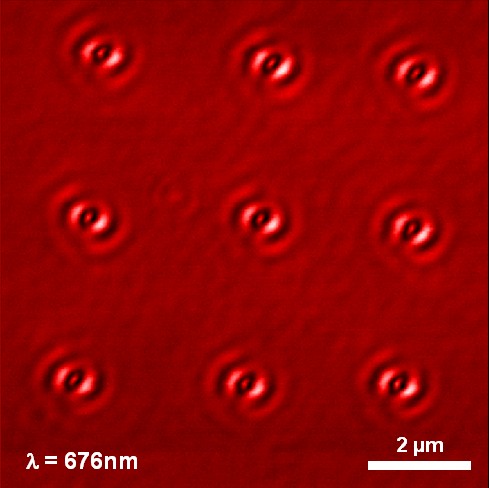
This image shows a near-field microscopy measurement of a sample used in our perfect lens studies. The ripples observed here are surface plasmons excited using our microscope, and scattered by nine platinum particles desposited on the sample. Note the high resolution: the wavelength used is 676nm, but features smaller than 100nm are observed. More information on this measurement can be found in the paper "In situ experimental study of a near-field lens at visible frequencies".
|
|